
Research Policy
In the manufacturing and processing processes of electrical and electronic materials, there are many phenomena that occur on the material surfaces during the process. Understanding and controlling such phenomena can contribute to the creation of energy-efficient and high-performance electronic devices, as well as the efficient use of energy in the field of electrical and electronic engineering. In particular, the elucidation of the mechanism for the generation and suppression of atomic-scale “defects” that occur during semiconductor manufacturing processes is an extremely important topic as it directly affects the performance of semiconductor devices.
In our laboratory, we aim to understand the atomic-scale phenomena that occur on material surfaces during the synthesis of electrical and electronic materials and the operation of electronic devices. By elucidating the control methods for these phenomena and clarifying their impact on the characteristics of electronic devices, we hope to contribute to further advancements in electrical and electronic engineering. To efficiently advance such research, it is essential to improve the experimental techniques and analysis methods. We are developing methods to automate and robotize experimental procedures to reduce the burden on experimenters, as well as data-driven spectrum analysis methods using Bayesian estimation and exchange Monte Carlo methods.
Major research achievements to date
Research on Si thermal oxidation reaction process for semiconductor device fabrication
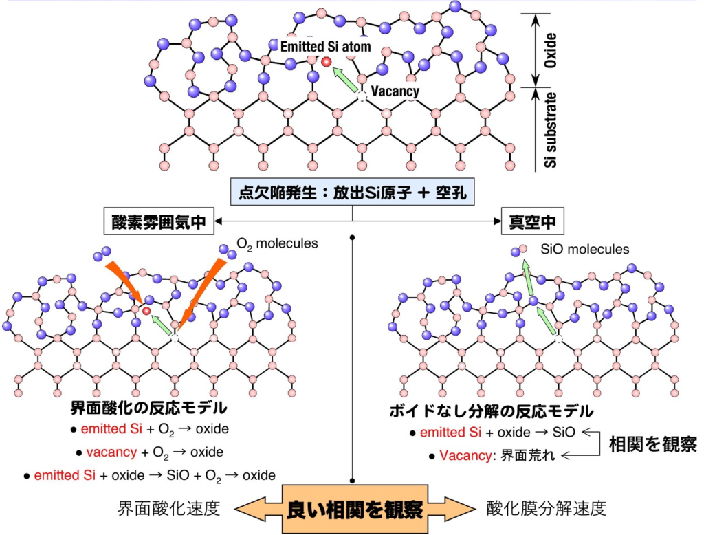
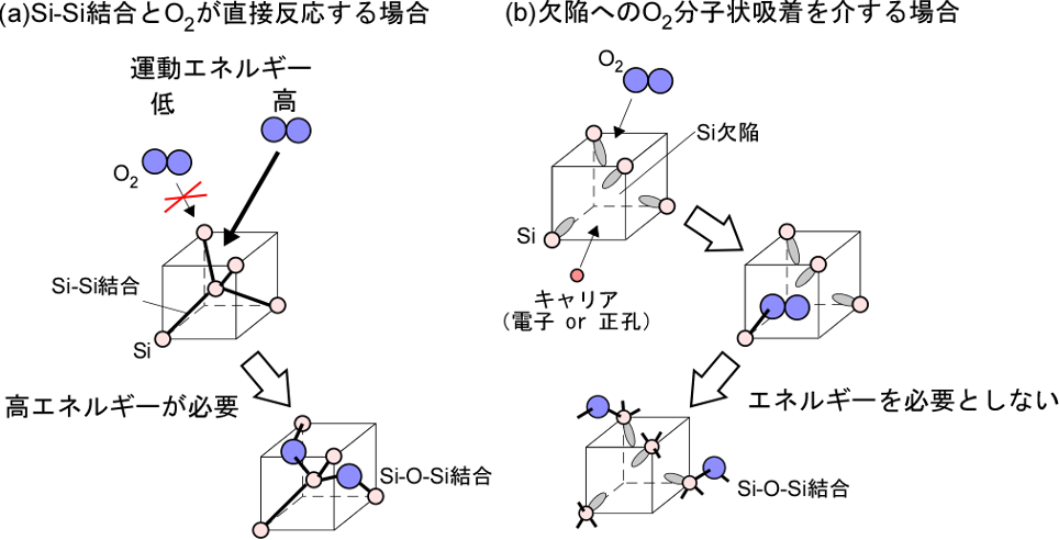
In the current semiconductor device manufacturing process, SiO2 is formed as an insulating film by thermal oxidation of the Si wafer. During the thermal oxidation process, not only SiO2 growth but also thermal diffusion of impurities doped in the wafer progresses. To suppress impurity diffusion, a “Rapid Thermal Oxidation (RTO)” process is adopted in which the wafer is rapidly heated and cooled during oxidation. Generally, chemical reaction rates are determined by temperature and concentration of the substance. However, the oxidation reaction rate by RTO could not be explained by conventional chemical reaction kinetics, and detailed elucidation of the reaction mechanism was required. To construct an integrated reaction model for Si thermal oxidation process, studies have been conducted using photoelectron spectroscopy and time-resolved photoelectron spectroscopy utilizing synchrotron radiation. As a result, it has been clarified that (1) the strain caused by the insertion of O atoms into Si-Si bonds drives point defect formation in the Si oxidation reaction [1, 2], (2) the unpaired electrons possessed by the point defects trap carriers in the semiconductor, promoting dissociation of O2 molecules [3], (3) point defects generated by strain are involved not only in Si thermal oxidation but also in the reduction reaction of SiO2 [4], and (4) efficient SiO2 film formation is achieved by RTO process due to thermal strain caused by temperature change [5].
[1] S. Ogawa et al., Jpn. J. Appl. Phys., 52, 110128 (2013).
[2] S. Ogawa et al., AIP Advances, 5, 087146 (2015).
[3] Y. Tsuda, S. Ogawa et al., J. Chem. Phys., 157, 234705 (2022).
[4] S. Ogawa et al., Jpn. J. Appl. Phys., 45, 7063 (2006).
[5] S. Ogawa et al., J. Chem. Phys., 145, 114701 (2016).
Development of carbon material synthesis method for next-generation electronic devices
Carbon materials such as diamond, graphene, and diamond-like carbon possess excellent electrical and mechanical properties as well as chemical stability, making them indispensable for realizing a carbon-neutral and hydrogen-based society. Depending on the application, carbon materials need to be shaped into single crystals, nanocrystals, thin films, etc., and the development of optimal synthesis methods for each shape has been necessary. Therefore, we have been conducting research on the development of high-quality functional carbon material deposition techniques and the elucidation of the operating mechanisms of functional films using carbon materials.
The first research achievement is the development of a conductive graphite deposition method onto an insulating substrate. Indium, which is a material for transparent electrodes, experienced a serious shortage at one point. To solve this problem, ultra-thin graphite films were investigated as alternative materials. In our laboratory, we were able to directly deposit low-resistance nanographite onto an insulating SiO2/Si substrate using photoemission-assisted plasma CVD [6]. Furthermore, we succeeded in directly depositing insulating amorphous carbon onto a single layer of graphene without destroying the graphene, by focusing on the fact that the photoelectron-controlled plasma CVD used for nanographite deposition is a low-damage process [7].
The second achievement is the construction of a microscopic model for the thermal CVD process on a Cu substrate. We applied the real-time photoelectron spectroscopy developed for Si thermal oxidation processes to the study of graphene thermal CVD processes on Cu surfaces. From the heating experiments of Cu substrates with graphene deposition, we proposed a model that suggests the presence of a carbon atom diffusion barrier film on the Cu surface during thermal CVD [8].
The third achievement is the discovery and elucidation of the mechanism of graphene’s selective molecular permeation function. In addition to studying the graphene deposition process, we have been advancing research on the functional evaluation of graphene in recent years. We discovered that graphene has a selective molecular permeation function that depends on the translational motion energy of molecules and elucidated its mechanism [9]. In particular, the discovery of graphene’s selective molecular permeation function has great potential for realizing a carbon-neutral society through the development of highly efficient hydrogen production catalysts and carbon dioxide reduction. We also investigated in detail the reactivation of Ni catalyst surfaces that had been deactivated by oxidation in order to utilize this graphene for the protection film of easily oxidizable transition metal catalysts [10].
[6] T. Takami, S. Ogawa et al., e-J. Surf. Sci. Nanotechnol. 7, 882 (2009).
[7] S. Takabayashi, S. Ogawa et al., Diamond Relat. Mater. 22, 118 (2012).
[8] S. Ogawa et al., Jpn. J. Appl. Phys. 52, 110122 (2013).
[9] S. Ogawa et al., J. Phys. Chem. Lett. 11, 9159 (2020).
[10] S. Ogawa et al., J. Vac. Sci. Technol. A 39, 043207 (2021).
Promote Dx of synchrotron radiation experiments through automation and AI of experiments and data analysis
In the field of electrical and electronic materials engineering research and development, a comprehensive exploration of material fabrication conditions is necessary. In particular, the synchrotron radiation facility, which is essential for evaluating synthetic materials, operates 24 hours a day, and experiments using synchrotron radiation have become commonplace, regardless of late-night or holiday schedules. As the decrease in the working-age population in our country poses a challenge, it is necessary to promote labor-saving and low-labor research activities in universities as well. The digital transformation (Dx) of the experimental and research process in the academic community is the means to achieve this. In the industrial sector, automation and robotization of manufacturing equipment are already common, and there is a large market for such technologies. On the other hand, equipment automation has not always been actively pursued in research and development settings. One of the reasons for this is that research and development involve what is called “multi-variety small-lot production,” which is incompatible with the automation technology required for “small-variety large-lot production” in general manufacturing. On the other hand, automating experimental work in basic research is expected to reduce the burden on researchers and technicians and enhance research and development capabilities. Therefore, it is crucial to develop automation technologies that match the needs of the research and development field.
Based on these backgrounds, we are advancing the development of a gas supply system that is also available at synchrotron radiation facilities [11], a method for detecting small peaks through a batch automatic analysis method for photoelectron spectra analysis that was previously carried out in separate processes [12], and an analysis program utilizing mathematical science models that are not dependent on the user’s experience or abilities [13].
[11] Y. Tsuda, S. Ogawa et al., J. Chem. Phys., 157, 234705 (2022).
[12] S. Ogawa et al., Appl. Surf. Sci. 605, 154748 (2022).
[13] in preparation.